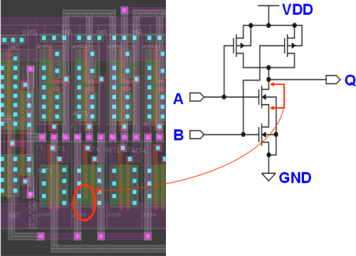
- DefSim Chip Layout
- Implementation of Defects
- Use cases
|
DefSim Chip Layout
|
|
DefSim chip consist of two blocks (HRDLIB and C17)
that contain matrices with various digital cells implemented.
For each cell there is a fault-free circuit and many
copies of the same cell with intentionally injected defects.
Additional circuitry, like multiplexers and decoders,
allow addressing and activating selected cells and
trnsmitting their responses. Only one circuit at a time
can be actived (selected).
The desired sort of defect can be activated by choosing faulty
version of the cell with the fixed (intentionally injected) defect.
To be close to the silicon reality each cell is loaded and driven
by standard non-inverting buffers. Since a built-in current monitor
was implemented in each block as well, it is possible to apply both
voltage method and IDDQ testing.
|
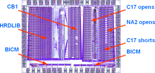
DefSim chip layout
|
List of Cells
Here we have listed circuits that were implemented in the chip.
The following gates were implemented using the industrial standard
cell library HRDLIB:
- AN1 = NOR( AND(A,B), AND(C,D) )
- AN3 = NOR( AND(A,B), C, D)
- EN1 = XNOR(A,B) = NAND( OR(A,B), NAND(A,B) )
- EO1 = XOR(A,B) = NOR( AND(A,B), NOR(A,B) )
- IN1 = NOT(A)
- NA2 = NAND(A,B)
- NA3 = NAND(A,B,C)
- NA4 = NAND(A,B,C,D)
- NO2 = NOR(A,B)
- NO3 = NOR(A,B,C)
- NO4 = NOR(A,B,C,D)
- NO42 = NOT( NAND( NOR(A,B) , NOR(C,D) ) )
- ON1 = NAND( OR(A,B), OR(C,D) )
- ON3 = NAND( OR(A,B), C, D)
- CB1 - Custom testability benchmark
DefSim chip also contains cells with C17 ISCAS-85 testability benchmark.
In both cases the layouts of CB1 and C17 were automatically synthesized.
|
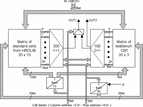
Schematic diagram of first block (HRDLIB) of DefSim chip
|
Implementation of Defects
DefSim integrated circuit contains a number of circuits including
fault-free circuits and their variations with
intentionally injected defects. There are two types
of defects implemented in DefSim: opens and hard shorts
in conducting layers (Polysilicon, Metal1, Metal2).
These defects are located both inside logic gates
as well as upon (or between) signal lines outside the gates.
Here we have examples of typical defects
implemented in DefSim chip:
|
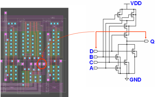
Complex cell with IN-OUT short caused by excessive Metal2 defect
|
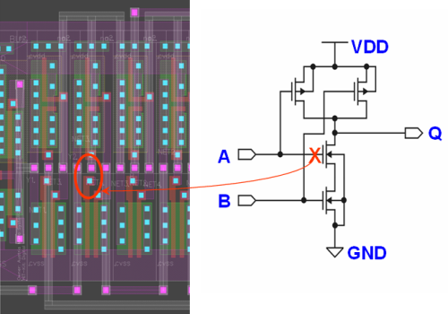
NAND2 cell with floating gate caused by missing Metal1 defect
|
NAND2 cell with Drain-Source short caused by missing Polysilicon defect
|
In general, the DefSim environment targets two
main challenges of testing: fault sensitization and
fault observability. Basically, the main questions
that can be answered by DefSim are:
- Which fault model is more efficient in describing existing defects?
- Does a particular fault model (e.g. Stuck-at Fault
or wired-OR) detect all defects in a given
Circuit Under Test (CUT)?
- Does one need to consider more than one fault model to cover all defects in a single given CUT?
In addition to that, the user can compare fault
detection (observability) efficiency of voltage
and IDDQ testing, obtain truth tables
of good (without defects) and defective circuits,
observe defect tables for available circuits, etc.
In the following we will consider several simple examples
of defects and discuss measurement data obtained for them
using DefSim kit.
|
Case 1 - Evaluating Stuck-at Fault Model
First of all, let's see if the Stuck-at Fault (SAF)
model covers all available defects for a selected circuit.
A complete SAF test for ON1 circuit given in
the table on the right:
|
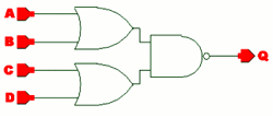
Complex gate ON1
|
| Test | DCBA |
| 1 | 0010 |
| 2 | 0100 |
| 3 | 0110 |
| 4 | 1001 |
|
Now we will pass the test sequence to the
DefSim hardware.
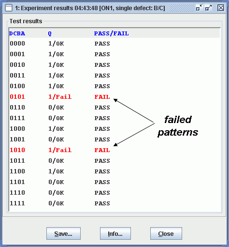
After running this test on DefSim hardware,
we see that two defects A/D and B/C were not covered:
|
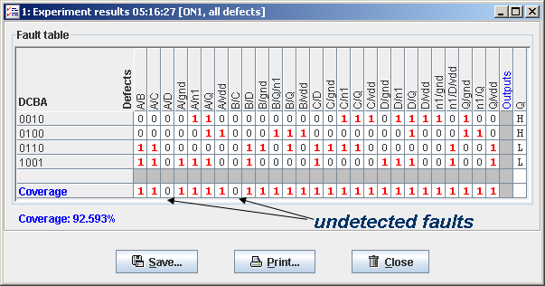
|
A/D and
B/C not covered!
Either 0101 or 1010 vector need to be added
|
In order to cover these two defects we need to add
either 0101 or 1010 vector:
|
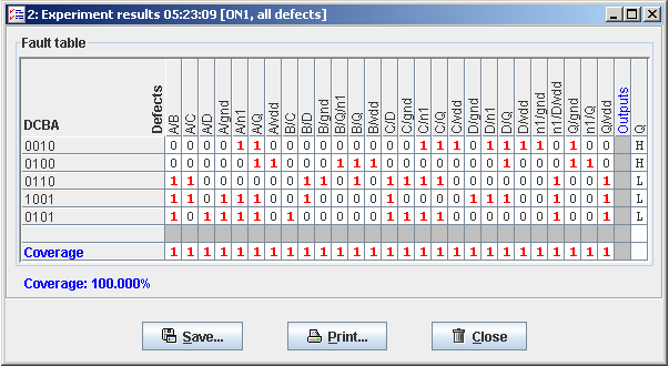
After 0101 vector adding to the test both
A/D and B/C
become covered!
|
This experiment shows that Stuck-at Fault model
sometimes provides insufficient fault coverage in real
circuits. This is a well-known fact of course, and
DefSim provides a very simple example that illustrates
this fact.
|
Case 2 - Bridging Faults: Wired-AND or Wired-OR?
Since, Stuck-at Fault is not an ideal fault model
for bridging fault detection we have to look at other models.
There are two common types of bridging fault models:
wired-AND and wired-OR.
For next experiment we chose bridging fault B/C
between ports B and C of the same circuit
ON1.
The goal of the experiment is to find
out which model (wired-AND or wired-OR)
describes given defect precisely.
Now we have to use both fault models and for each
fault model find all test patterns detecting defect
B/C.
Wired-AND model produces 2 patterns
and wired-OR – 4. These patterns are
presented in the table below:
|
Complex gate ON1, defect: B/C
|
| Test |
Wired-AND |
Wired-OR |
| DCBA |
DCBA |
| 1 |
1010 |
1100 |
| 2 |
0101 |
0100 |
| 3 |
|
0011 |
| 4 |
|
0010 |
|
|
Now we can evaluate all test patterns by using
DefSim environment.
Measurement results concerning their detection
of a given defect (short B/C) are
presented below:
|
|
Wired-AND model describes this defect
|
Here we can see that measurements fully agree with
wired-AND fault model.
|
Case 3: Victim-agressor Model
Although, wired-AND is the most common model used for
bridging fault modeling in CMOS technology, it is not always
relevant. Let's consider short D/Q now, i.e. the
fault between input and output. Wired-AND and
wired-OR test patterns for this short are
given the table below:
Complex gate ON1, defect: D/Q
|
| Test |
Wired-AND |
Wired-OR |
| DCBA |
DCBA |
| 1 |
0000 |
0001 |
| 2 |
0001 |
0010 |
| 3 |
0010 |
0011 |
| 4 |
0011 |
1001 |
| 5 |
0100 |
1010 |
| 6 |
1001 |
1011 |
| 7 |
1010 |
1101 |
| 8 |
1011 |
1110 |
| 9 |
|
1111 |
|
|
Now, let us analyze results of measurements that
were performed using DefSim:
|
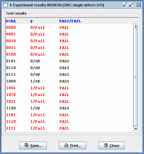
|
Neither Wired-AND nor Wired-OR?
Victim-aggressor behavior: A is a stronger driver!
|
|
One can easily see that in reality more patterns detect
D/Q short than predicted by either wired-AND
or wired-OR model. After some analysis, it can be
seen that the fault is always detected when D is
different than Q, which means that output Q
always takes the value of D.
In other words, the buffer that drives input D
is a stronger driver than the output Q of the
complex gate ON1.
There are many more interesting experiments possible to
run with DefSim measurement environment.
For example, some opens implemented in DefSim
cause memory effects in the circuits.
|
|